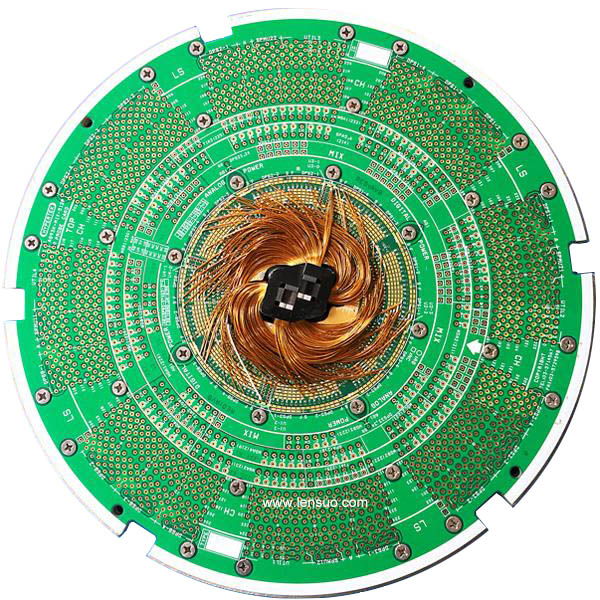
Product Name: probe card PCB
Plate: Panasonic M6
Minimum DUT pitch: 0.65mm
Surface technology: nickel palladium
Plate thickness: 4.0 mm
Number of floors: 28
Copper finished product size: less than 18 * 24 inches
Purpose: probe card PCB is used to connect the tester and pad on die
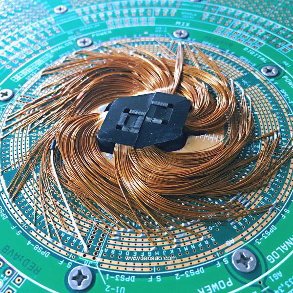
The probe card is used to test LSI (large scale integrated circuit) chips on the chip during the wafer testing process in LSI (large scale integrated circuit) manufacturing process. The tester is connected with the chip.
The probe on the probe card is in direct contact with the pad or bump on the chip, leading out the chip signal, and then cooperating with the peripheral test instruments and software control to achieve the purpose of automatic measurement. The probe card is used before IC packaging. The function of the probe is tested for the bare crystal system, and the defective products are screened out and then packaged.
Wafer testing process is very important and highly dependent on the reliability of probe card.
Material specification Click
Panasonic M6 r-5775 (n) & r-5670 (n) specifications
We always adhere to the "integrity-based, quality first", the principle of. The establishment of long-term, stable partnership, is our eternal goal. Some more information, please contact our: sales@fjhnxc.com
Quick response
 0.5H quotation, 1H engineering response, 24H customer service,24H technical support.
Stable quality
 LENSUO always adhere to the customer's trust with good and stable quality win if you just.