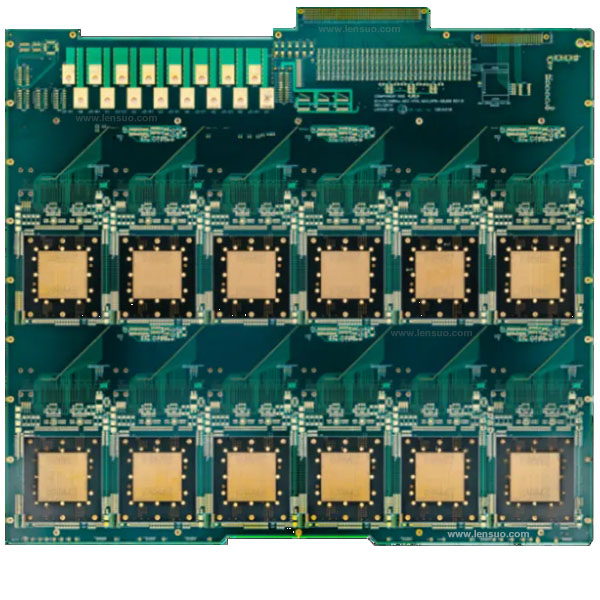
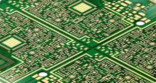
Product Name: BIB (Burn-In Board) PCB
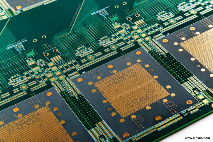
Plate: fr - 4 High Tg ( Tg 175 )
Plate thickness: 3 . 2mm
Surface technology: Shenjin 3U
Number of layers : 20th floor
Copper thickness : Inner layer 70 / 35um , Outer layer 35um
BGA number : 24
Dimensions : 610 x 572 mm
Purpose: IC BIB (Burn-In Board) PCB
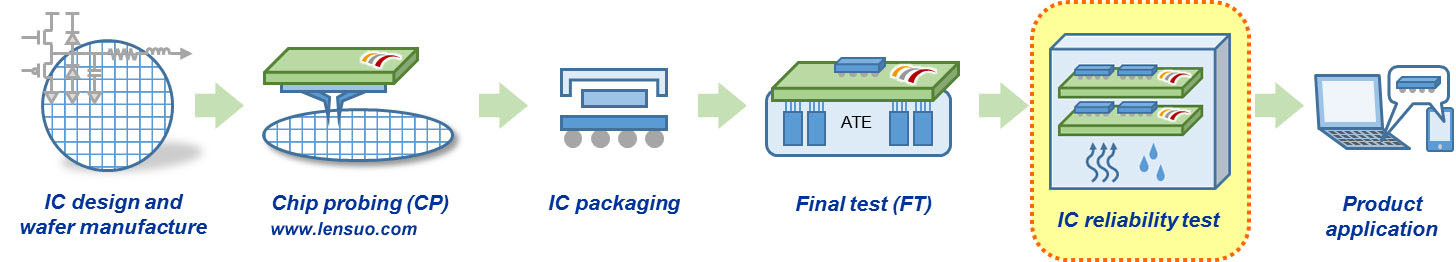
As the carrier of semiconductor IC, IC bib (burn in board) connects the IC that needs to be tested with IC bib (burn in board) through socket or other ways, and puts it into the testing machine to test different temperature, voltage and signal of IC, so as to check the reliability of IC.
BIB (Burn-In Board) PCB:
(1) HTOL test (high temperature operation life)
HTOL is mainly used to simulate the life test of IC in high temperature environment with continuous power on (voltage or current added). It is used to detect whether the functionality and characteristics of IC will change due to environmental conditions, and evaluate the long-term operation life of IC.
(2) Hat test (high accelerated stress test)
When the IC is exposed to extremely high temperature and humidity, it will accelerate the water vapor to penetrate into the IC through the interface between the external protective material and the metal wire, so as to evaluate the humidity resistance of the IC structure.
Lensuo is a manufacturer of bib (burn in board) PCB, which provides professional manufacturing services for bib (burn in board) PCB.
Lensuo has many years of PCB design and manufacturing experience in IC carrier board and IC test board. It can provide the best circuit design for customers and complete electrical RF / Si / PI simulation service in the design stage.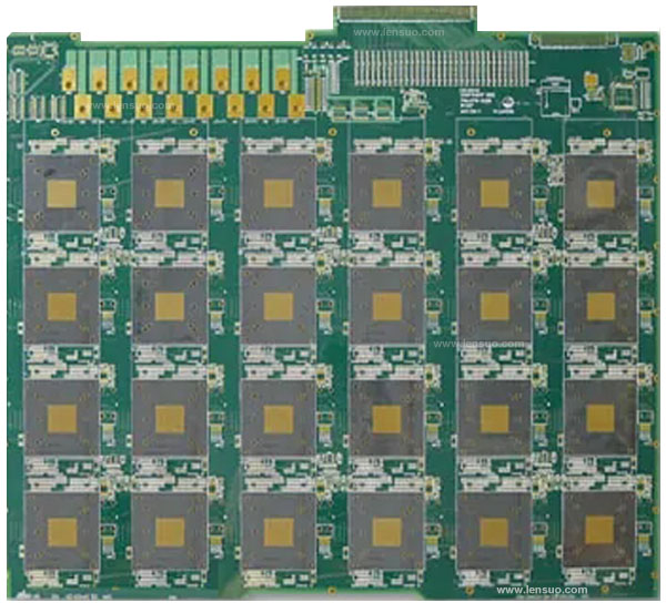
Requirements of bib (burn in board) PCB:
1. In order to prevent chip power supply or signal short circuit from causing other chips unable to work, each chip needs independent power supply, which is connected with the main power supply through resistance.
2. When the current of wiring is greater than 500mA, it shall be indicated in the schematic diagram.
3. If the high frequency wiring has impedance matching, the thickness of copper foil, line width and PCB material should be given.
4. Sensitive ports and devices that need shielding or other special treatment shall be clearly marked.
5. Crystal oscillator circuit needs to give a typical application circuit, including its matching capacitance value.
6. It is necessary to specify whether analog circuit, digital circuit and pavement need to be partitioned or divided.
7. If the signal source needs to be provided from outside, the driving ability and relevant indexes of the required signal source are given.
8. PCB board has no abnormal deformation and distortion under high temperature (150 ℃) for a long time.
9. PCB circuit will not have any short circuit or open circuit due to high temperature environment.
We always adhere to the "integrity-based, quality first", the principle of. The establishment of long-term, stable partnership, is our eternal goal. Some more information, please contact our: sales@fjhnxc.com
Quick response
 0.5H quotation, 1H engineering response, 24H customer service,24H technical support.
Stable quality
 LENSUO always adhere to the customer's trust with good and stable quality win if you just.